I Always Wanted to Build A Receiver
SPECIFICATIONS
Bands: 80 thru 10 meters
Modes: Image Reject or Binaural
Audio bandwidths: 2 kHz or 500 Hz (image reject); 4 kHz binaural
Noise Figure: 19.4 dB
Input IP3: +21.5 dBm
MDS: -128 dBm
To get myself back on the air, I decided to start with a homebrew receiver. This project took about 15 months, beginning October, 2005. It covers the HF bands and is based on two important building blocks, the KK7B R2Pro direct-conversion receiver and the AA0ZZ IQPro DDS (direct digital synthesis) VFO. These basic designs I modified and then added features to suit my needs. So here's the full story... It's quite long!
Here are the basic modules:
RF low-noise amplifier (LNA) and bandpass filters
IQPro DDS VFO
R2Pro downconverter
Audio signal processing
Fabrication Techniques
The main modules are fabricated from brass sheet, mostly 50 mil thick. I have a machine shop, so I can mill parts to any size with accuracy. Note that there are no fasteners on the front panel. That’s because I machined numerous threaded brass standoffs which are soldered to the back of each panel. All the enclosures are soldered. I use an oxy-acetylene torch for most of the soldering because it heats a localized area quickly, thus avoiding a complete “meltdown” of the entire project!

The case is made of 1/2-inch birch plywood. The plywood is covered with 1/16-inch veneer cut on my bandsaw from a plank of peruvian pine, a fairly rare wood. I lined the inside of the cabinet with 3-mil copper foil, glued in place with spray adhesive. The rear panel is aluminum.
Except for the IQPro kit, all the circuits are built on pre-etched circuit prototyping board material. My favorite pattern has a ground plane and a 1/10-inch grid of plated-thru holes to individual pads (Twin Industries 8100-410, from Digikey). This gives me the advantage of having all that ground plane area and something with a nice grid into which all the parts are soldered. It’s great for small/quick prototypes, but also makes a robust finished product for the hobbyist.
What’s Inside
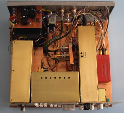
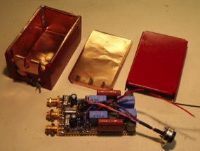
The little red box at the far right is the R2Pro downconverter. At the upper left is the power supply, which has a toroidal transformer with the usual rectifiers, filters, and three-terminal voltage regulators. In the center of the chassis is a small module containing output buffer amplifiers for the I and Q oscillator outputs that are routed out of the chassis to the transmitter.
The basis for the whole receiver is the R2Pro by Rick Campbell, KK7B. You can find information on it in his book, Experimental Methods in RF Design, and on the web. Kits are long discontinued, unfortunately.
RF Front-End
The front-end consists of a low-noise JFET amplifier with bandpass filters, exactly as designed for the R2Pro, which I upgraded to a multi-band front end. In consultation with Rick, I used five separate LNAs, followed by a buffer amplifier and attenuator. This extra stage provides a very stable 50-ohm source for the downconverter’s mixer. There is also a step attenuator right after the antenna for use when signal levels are extremely high.
I wrote two reports on this work that will tell you more than you want to know about front ends of this type. Part one covers the requirements and has lots of measurements on the basic JFET LNA. Part two covers the buffer amplifier and shows the overall performance as a system.
Since other folks are interested in multi-band applications of the R2, I teamed up with Craig Johnson, AA0ZZ, who went forth and laid out a beautiful circuit board. It’s a modular design that has space for two bands on a single board with an option for stacking several more for multi-band use. He also includes lowpass filters for a mating transmitter (up to about 100 W class), and decoding logic for automatic bandswitching when used in association with his IQPro DDS VFO (see below).
I built mine ugly style and stuffed it in the brass box shown below. Craig’s board set is much better but came along later. Electrically they are the same but mine doesn’t have automatic band switching. My S meter is mounted in the front panel; more on that later.
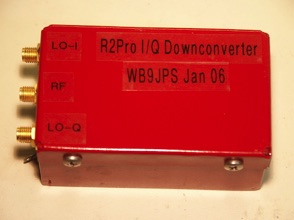
An I/Q Downconverter
This circuit is nearly identical to the original KK7B R2Pro downconverter design. I used a slightly higher-level mixer (13 dBm rather than 7) which generally improves dynamic range. I used a Mini-Circuits splitter (TSC-2-1) instead of a hand-wound unit. Transistors are 2N4401 rather than 2N3904 because their noise figure is slightly better; the ‘4401 is an old secret in the audio business. Finally, I used an emitter follower at the output rather than a final gain stage. My next stage has a low-noise instrumentation amplifier at its input, which is provides needed gain while rejecting common-mode noise and also breaking up ground loop hum.
I re-biased the circuit slightly to optimize return loss at the input to the common base amplifier. To do this, I used a resistive return loss bridge that was described in the 1996 ARRL Handbook. That way, the diplexer is accurately loaded at all audio frequencies.
By the way, I did experiment with several other amplifiers. Candidates were: a common emitter amplifier with two transistors in parallel; a common base but with two transistors in parallel; and a couple of low-noise opamps (AD787 and LT1028). Slightly lower noise was achieved with the dual-transistor common emitter circuit but at the cost of much higher complexity, especially a number of large electrolytics. It is, in fact, hard to beat a noise-matched common base in this application, especially if you want to avoid a very high parts count. And besides, it’s a case of diminishing returns. Even a noiseless amplifier would not significantly improve the noise figure of the complete receiver.
Other Little Features
The diplexer was tweaked for a nearly-perfect 50 ohm match from dc to over 100 MHz. A simple improvement you can make even without a return loss bridge is to compensate for the dc resistance of the last big inductor that goes to ground (~33 mH). Connect an ohm meter in place of the mixer IF output, and adjust the resistor in series with that inductor until you get 50 ohms.
Power supply rejection is enhanced by including a local voltage regulator. The LM317 is a very common part and actually has about as good a noise level as you will find. Remember that this is an audio amplifier, and your direct-conversion receiver has enormous gain. That means any power supply noise gets amplified by something on the order of 100,000 times!
The output goes through a mini-DIN connector. Since the audio feeds a differential amplifier, I used a balanced RFI filter consisting of a common-mode choke and a couple of capacitors.
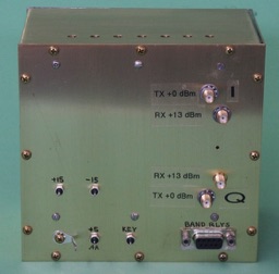
The enclosure is fabricated from welded 1/8 inch steel plate because the inductors make this circuit susceptible to hum pickup, so ferrous shielding is advised. The box is lined with thin copper foil to provide a really good RF shield, especially where the cover meets the body of the box. SMA jacks are tightened after the box is closed up, so all the shielding and the connector grounds are very well clamped.
From left to right, the main boxes are
RF low-noise amplifier (LNA) and bandpass filters
IQPro DDS VFO
Audio signal processing
About Hum Pickup
It’s a fact that large inductors in audio systems are susceptible to local magnetic fields, and the very high gain of a receiver system aggravates the problem. I first discovered I had a hum problem when I gathered all the receiver modules together, near the power supply. Even though the downconverter is magnetically shielded, and the power transformer is toroidal and enclosed in a steel box, 60 Hz harmonic buzz was clearly audible. Here is the power spectrum of that noise:

Trying to measure minimum detectable signal sensitivity is almost meaningless with all this buzz. The situation was remedied by moving the downconverter to the far opposite corner of the receiver chassis; distance is your friend when it comes to magnetic (or electrostatic) coupling.
I had a conversation with Rick, KK7B, about this. His answer is simple. The R2-series receivers were primarily designed for battery power operation. Or, you run it on a well-filtered dc supply located several feet away. In either case, you have removed the source of the intense magnetic field and all is well. So be warned! Don’t put this downconverter right on top of a big transformer...
IQPro DDS VFO
My VFO is the IQPro DDS VFO kit designed by Craig, AA0ZZ. It's based on the AD9854 DDS chip, with a couple of PIC microcontrollers. It’s very versatile, with a nice user interface, and covers the 1.8 to 30 MHz range that I needed. The quadrature outputs are a perfect match to the R2Pro downconverter; all you have to do is match the output levels. Craig did a great job on the overall architecture (it’s a second-generation design), and he’s especially good on the software aspects..

Customization and Characterization of the VFO
I started making measurements on the IQPro and decided that the way to get the high-level output I wanted, with low distortion, was to use wideband opamps. The IQPro has, as an option, transformer-coupled outputs, which are just fine and provide about +3 dBm. I did a bunch of measurements, and then characterized a variety of candidate opamps before finally settling on the LMH6703 to provide +13 dBm. Here is the report: IQPRo_Performance_and_Wideband_Opamps.pdf
Construction
All parts of the enclosure were fabricated from 0.050 brass sheet, folded and soldered, with 0.187-thick brass strips soldered along edges where I needed to drive screws. That’s thick enough to tap #2-56. Standoffs for various boards were machined from brass rod. Finishing consisted of wet sanding prior to and after assembly, with some help from a hot ammonia soak to clean up corrosion in dark corners. To keep things shiny, I use Staybrite spray lacquer designed for brass, available from Woodcraft. Hand lettering was done with a Rapidograph #2 pen with ink that is meant for mylar. I also used some clear stick-on labels from one of those cheap label makers for the buttons.
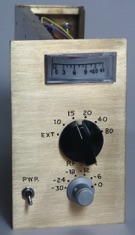
The front panel was drilled on a vertical mill to obtain a uniform pattern that exactly matches the Vector board that holds the pushbuttons and LEDs. The knob was turned from aluminum; it has a knurl on the side. The display bezel is aluminum. I thought the contrast would be nice against brass. The box is 5.0 inches tall. I use that as a standard dimension for the modules that will make up the rest of my receiver.

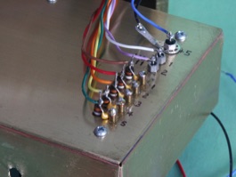
All the power was brought in via feedthrough capacitors. I got most of them from Mouser (Spectrum Control). Band relay digital outputs went to a DB-9 jack. Filtering for those was discussed on the DDS-VFO Yahoo group (msg. no. 2864). I used 220 ohms in series with each lead, and 10 nF to ground. RF signals come out thru SMAs.
Vent holes are drilled on the sides and top. Holes in the top line up with similar holes in the RF section inside.
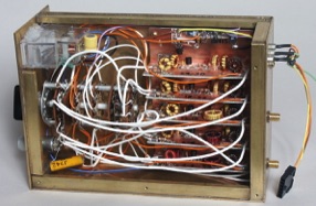
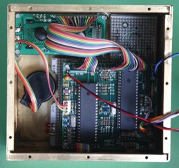
Looking inside the main box from the back, you can see that the IQPro CPU board is floating above the switch/LED board on standoffs. Standoffs for the switch/LED board and the LCD display are soldered to the inside of the front panel so there are no visible fasteners. To align them, I made sheet metal templates with holes that match those in the boards. Then everything is clamped in place while soldering. The front panel was completed before soldering it to the sides. After the enclosure was all soldered, I mounted it on the mill table and took a final cut on the back to give the rear panel a nice flat mating surface. I suppose I could have gone haywire and added RF gasketing, but this is only for the HF bands.
A sub-enclosure houses the RF section, and it bolts onto the rear panel. You can see the SMA connectors that feed through the rear panel. Everyone who uses these DDS chips knows how hot they get. I glued on a small heatsink with a metal-loaded epoxy. That made a big difference, and it’s even more important with the very limited convection cooling in this enclosure (there are holes along the top and bottom).
You can see the IQPro RF board, mounted on standoffs. Its outputs go through subminiature Teflon coax that I had lying around. The first board it reaches contains a pair of 3 dB hybrid splitters and some voltage regulators. One side off each splitter routes the signal to an output for a transmitter (0 dBm out), and the other goes to the booster amps that drive the receiver’s mixers. Those amplifiers are LMH6703s on their evaluation boards, and they deliver +13 dBm. Power is ±6 V from a pair of regulators located on the power splitter board. Prime power is ±15 V for the amplifiers, and 5 V for everything else.
To get the SPI bus digital control signals into the RF section while rejecting some RF leakage, I used an RC filter. There was a thread on the DDS-VFO group called Driving DDS with Feedthru Caps, if you want to read all about it. Here’s the deal: The IQPro has CMOS digital outputs, and we need the transitions to be relatively fast and clean, otherwise the DDS chip will not understand the bit stream. And the CPU swings 5 V while the DDS can only handle 3.3, so there is a voltage divider on each pin. By reducing the default resistor values from 5.6K and 3.3K to 560 and 330 ohms, we can supply enough current to drive perhaps 1 nF of bypass capacitance. That could be a feedthrough capacitor.
But there’s an additional problem. Depending on how long the wires are and how they are routed, you can end up with crosstalk. Or, the resulting risetime may be marginal for your particular DDS chip. In my case, I found that it was impossible to get reliable operation with 1 nF feedthrus. By the way, the tolerance on many feedthrus is awful. My 1 nF units were more like 1.8 nF. So the solution I came up looks like this:
I chose 470 pF because it was as large as I could go with reliable operation. The resistor increases the source impedance looking into the RF box, which gives us a more favorable voltage divider at several MHz, thus enhancing the suppression of RF leakage. Meanwhile, the resistor doesn’t slow the risetime much more because the input capacitance of the DDS chip is very low. Also, the resistor make a nice insulated feedthru terminal. I use 1/2 watt carbon in a tight-fitting hole. A dab of epoxy makes it permanent. Since the panel is rather heavy, I added #4-40 brass screws at each feedthru location and used them as solder lugs for the bypasses.
Total power consumption is about 380 mA from 5 V with the backlight on. Current on the ±15 V supplies is something like 60 mA. It works great. Thanks to Craig for a nifty kit. It’s been a great ride.


Audio Signal Processing (ASP) Box

After the downconverter produces a quadrature pair of baseband (audio) signals, the ASP does the actual demodulation. The most important mode is image-reject SSB demodulation by the phasing method. This is fully explained in the R2Pro receiver writeups, and my implementation follows those designs almost to the letter. What I did differently is to use opamp-based active filters instead of LC filters. I won’t show all the schematics here because such filter designs are routine.
At the input end of the ASP, I used INA128 instrumentation amplifiers to reject common-mode noise and to break up any ground loops. This is a very powerful technique, useful when you need to ship audio signals around between boxes.
Next, I included a recommended phase balance adjustment. That, in conjunction with the usual gain balance, allows you to optimize alternate sideband rejection. I put the pots on the front panel and made a little table of settings for each band. It’s simple and effective.
My receiver also has a binaural mode, another of KK7B’s contributions (QST, March, 1999, and reproduced in the ARRL Handbook). This is a fascinating kind of receiver to listen to because your ears are fed the raw quadrature signals, which produces a very cool spatial representation of all the signals near the VFO frequency. It’s fun when you want to quickly tune around the band and see what’s happening. It’s also a great way to find perfect zero beat on a carrier, like WWV. As you approach zero beat, you hear the sound swirling and bouncing between your ears, gradually slowing to a stop when you’re right on.
The volume control is a dual linear pot (RV4N) modified for quasi-log response. A nice article on potentiometer responses is available here.
After the highpass filter, there is a muting switch (FETs), and then the final stage is a summing amplifier where the sidetone is injected.
Sidetone Oscillator
A good sidetone is a clean sinewave at your favorite frequency, and it should switch on and off without clicks. The one I chose is based on simple a twin-T oscillator running at low voltage and low current to limit the transistor’s gan-bandwidth product. It produces pleasingly low distortion and noise.
The first thing you have to do is avoid coupling any changes in dc level to the audio output when switching between transmit and receive. If you study the schematic, you’ll see a .47 uF capacitor before the T/R switch and volume control. That’s all it takes. Don’t put the coupling cap after the switch!
The other thing you must avoid is suddenly turning the oscillator on an off, which generates nasty transients, identical to key clicks. I used an RC combination to limit the slew rate of the T/R control signal that operates the 2N7000 switching transistor. The result is a crisp and click-free sidetone with a modest parts count.
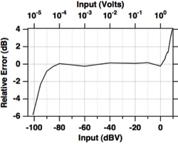
An Accurate S Meter
I designed an accurate S meter for this receiver, and it works great. It’s based on an AD8307 demodulating log amp, operating on the audio signal. It was published in QST, February 2008, p. 33-36. Due to copyright rules, I can’t supply a copy of that article. But I’m more than happy to answer questions.
Here is a graph of the S meter’s response error. For a ±1 dB error band, it achieves a 96 dB dynamic range.
What’s Next for the Receiver?
When I finished the initial build, that was pretty much it and no further work was done. A number of features were left off including power amps to drive speakers and AGC. No big deal. The main thing was the process of building a wonderful radio, and the fact that it sounds great!