One of the most desirable instruments in the RF engineer’s arsenal is a vector network analyzer. It gives you the ability to directly measure all of the key parameters of two-port networks, such as gain and return loss. The one I’m building was conceived by Paul Kiciak, N2PK. He’s a very talented RF engineer and has given the amateur community an amazing new capability. There is a group for the N2PK VNA (membership required). There, you can see info from many happy builders.
It’s based on a pair of DDS generators (RF and LO) and a direct-conversion, or zero-IF, detector with a 24-bit ADC. It’s a unique approach that is simple and yet offers absolute accuracy and dynamic range equal to or better than commercial analyzers over its 60 MHz range. A transverter may be added to expand the frequency range. For now, I’ll stick with the basic unit.
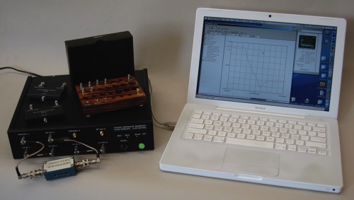
The instrument itself contains no intelligence; rather, a PC talks directly to the hardware via SPI and digital I/O bits via a parallel port connection. Mine has a USB interface, designed by G8KBB, and available commercially from Elrasoft. I usually run my own application software on my trusty MacBook.
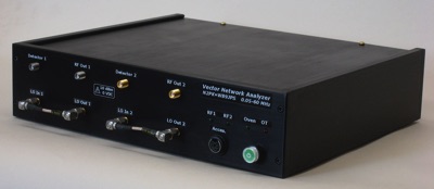
About My Build
Features of my particular VNA include:
• Dual detectors
• Ovenized main VNA board
• USB interface
• RF output switching and step attenuator to support full S-parameter test set
• External 12 VDC power
• Front-panel accessory power jack to support external amplifiers, etc.
• Machined and anodized aluminum enclosure
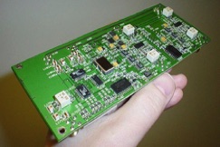
The PC board I’m using contains two detectors, which will support a full S parameter test set. Even without the test set, this enables simultaneous measurement of, for instance, gain and input return loss. The board is available from Ivan Makarov, VE3IVM. Ivan’s site contains also a great deal of practical information on the VNA.
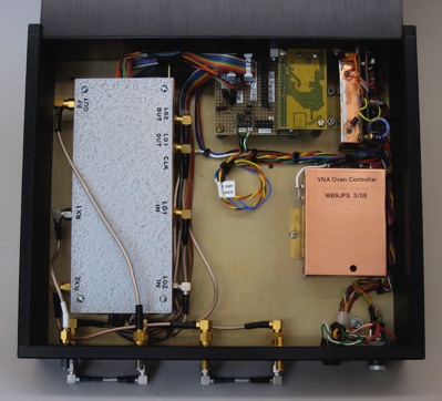
Enclosure
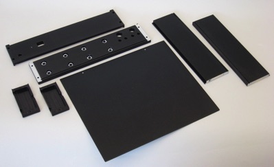
Since I have a basic machine shop, I enjoy fabricating mechanical parts for my projects, so I decided to make a heavy aluminum enclosure for the VNA. Walls are .375” 6061-T6, the bottom plate is .125”, and the cover is .063”. Parts were anodized black through the help of a local machine shop that we do business with. The owner was wiling to add my small batch of parts to a bigger job gong to the platers, so the work only cost me a bottle of Merlot. When anodizing, you can ask them to mask off parts where you want to maintain electrical contact, including the inside of tapped holes.
The bottom plate is Alodined. I got my Alodine materials online from Aircraft Spruce and Specialty Co. but there are certainly other sellers. Preparation starts with sanding with a belt sander, and also some hand wet-sanding with P120 grit silicon carbide paper, followed by a detergent and water wash. Next, the part is cleaned with Metal Prep #79, a phosphoric acid etchant. That has to be thoroughly rinsed in water. While it’s still wet, the part goes directly into the Alodine #1201 Solution. I use a shallow pan with just a few ounces of solution in it for each of these steps, and a wide paintbrush to apply the solution while the part stands on edge. Keep turning the part so the solution runs over it from all directions, otherwise you will get streaking. The Alodine step takes about 10 minutes, and leaves a golden brown color that is conductive with excellent corrosion resistance, even outdoors. It is also an outstanding preparation for painting. I will never make another aluminum part that goes without this treatment, except if it will be anodized. By the way, for anodizing, I sand the parts very carefully to 120 grit and VERY thoroughly wash them. What you see is what you will get; anodizing makes odd scratches and nicks stand out!
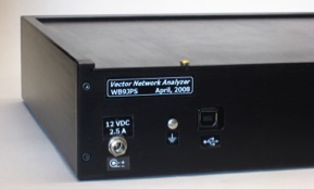
Panel labels are white-on-clear, made on a Brother labeler. I have one of their models with USB that allows you to paste in graphical items, like the USB and ground symbols I put on the back.
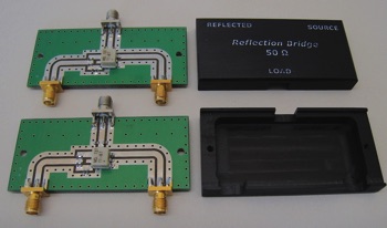
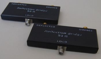
Reflection bridges, also built on boards supplied by VE3IVM, are fitted to small machined housings. This adds mechanical reinforcement to the end-launch SMA connectors and provides a bit of shielding. I tried out a silkscreening kit for the labels on this, with mixed results. Using their finest mesh yields clear edges on text down to about 9 point, but there are some clogging problems during developing that I was never able to overcome. Also, the kinds of stenciling inks available to the amateur are not as resistant to wear as the commercial stuff, which is incredibly expensive. So I’ll be “sticking” with labels for now.
An Oven for the Main Board
A number of components are somewhat susceptible to temperature drift, so I decided to ovenize the main board. Why ovenize? The VNA is a metrology instrument where absolute accuracy in amplitude, frequency, and phase are always important. Because the main board is so small, it is practical to put the whole thing in an oven. (That, and because I’ve done this before, it’s not such a big deal.) The result is an instrument that is repeatable to the part per million level or better, in all specifications, regardless of ambient temperature.
There is a technique the N2PK VNA group is calling corellated double sampling (CDS) that cancels offsets and 1/f noise in the detectors. It’s a software-driven technique that is now implemented in the the available VNA software, and is discussed in the VNA Yahoo group. The only drawback is that it doubles the scan time. It also can’t help with other sources of error such as gain or frequency drift elsewhere in the system, but it does a great job of improving dynamic range. Without an oven, CDS offers vast improvements. With an oven, it’s only necessary for measurements with the highest demands on dynamic range.
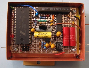
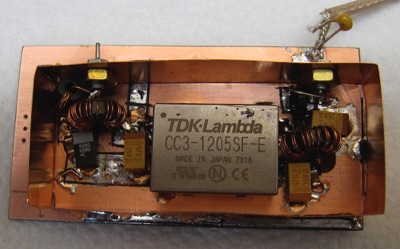
The oven system begins with a set of 8 short brass bosses soldered to the ground plane of the board to improve heat transfer to a copper heat spreader. It all resides in an insulated copper housing. Thin-film heaters are applied to the heat spreader, and thermistors are glued to the sensitive areas of the board. A Zilog Z8 Encore XP microcontroller measures the temperature and adjusts heater current through a PID algorithm.
I tested everything out before loading the board to obtain a good model of the process and to develop a good set of PID tuning parameters. This I did with LabVIEW and a National Instruments PCI-6035E data acquisition board. This allowed me to measure several temperatures and drive the heater’s constant-current source with a PID algorithm. Then I translated the LabVIEW code to C running on the Z8. Since the code runs slowly (2 Hz loop rate), all computations are single-precision floating point, which makes programming very easy.
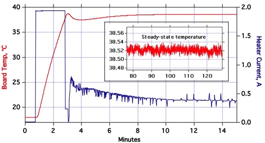
The graph below shows the startup performance with an inset showing fully-settled stability with a noise band of ±0.02 °C. Startup is quick because I use a computed ballistic heatup algorithm where the heater is turned on at full power until observed temperature reaches a specified error band. Then the PID engages with only a relatively small error to deal with. In 8 minutes from application of power, temperature is within 0.1 °C of setpoint.
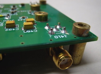
Closeup of tapped brass bosses soldered to the bottom of the board. There are 8 of these to provide good thermal grounding to the enclosure’s copper heat spreader. Their dimensions are 0.250” dia, 0.200 long, and tapped #4-40.
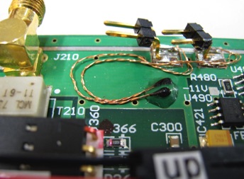
Two 10k, 0.5% thermistors were epoxied into place on the top ground plane. One is used for control, the other for monitoring during controller tuning. Several others were taped to various other locations during testing to verify that thermal gradients are very low, on the order of 0.1 °C between the two detectors.
Here is the VNA board nestled in the bottom of the heater box/shielding enclosure. The horizontal wall below connector J360 is a shield for the second detector channel.
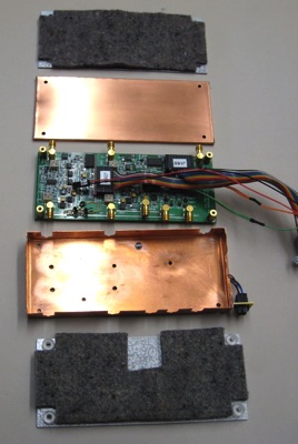
All the oven parts laid out. Insulation is heavy felt, good enough for the moderate temperatures. Small pieces are also placed on top of the board to reduce convection currents inside.
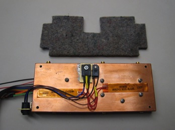
All heater components reside outside the VNA enclosure to minimize chances of noise coupling. I used a power darlington and a pair of Minco thin-film heat strips (each rated 13 Watts), attached to the copper heat spreader. There’s also a 70 °C thermal switch to cut off the power in case the controller fails.
The Z8 controller and thermocouple signal conditioner reside in an RF-tight copper box with feedthru capacitors. All heater components reside outside the VNA enclosure to minimize chances of noise coupling.
Power Supplies
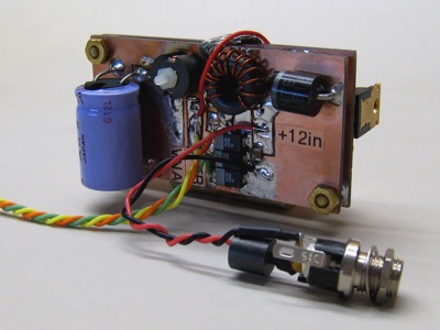
External power comes from a regulated 12 VDC, 2.5 A modular supply. I verified that this switching supply is pretty quiet with only about 2 mV rms ripple at 150 kHz, plus harmonics. There are two stages of passive LC filtering before the 12 V heads for the VNA board. 5 V is provided by an LM7805 bolted to the back of the chassis.
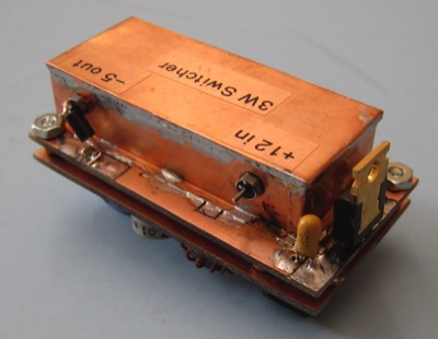
I also added a -5 V, 3 W switching supply for use with wideband opamps that I generally use for buffers. That supply (TDK CC3-1205SF-E) has a high switching frequency (700 kHz), is well-filtered, and resides in a soldered-up box with feedthru capacitors. Residual noise could not be detected on my spectrum analyzer without a low-noise preamp, with the only detectible peaks being less than 1 µV at 7 MHz. Now that’s quiet!
USB Interface and Digital I/O
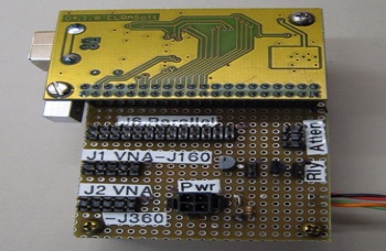
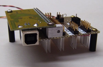
The Elrasoft USB interface board plugs directly into a wirewrapped fanout board that I made on perfboard for distribution of digital signals. I prefer double-row 0.1 inch headers since those are usable with mass-terminated cables. This board also has the driver transistors for the RF relays and attenuators that are part of a full S-parameter test set.
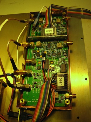
Below is an overview of the completed chassis, without the test set modules which are still in development. Interconnects are SMA jumpers that I got on Ebay--a really good deal--but watch out because a few of them had not been crimped!
S Parameter Test Set for the N2PK VNA
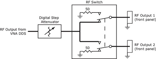
A full-featured VNA has a test set that allows you to fully analyze a device under test (DUT) without manually reversing its connections. This requires a high-quality RF switch. Another useful feature is a digitally-controlled RF attenuator so that you can set the drive levels differently for forward and reverse tests. Finally, a couple of bias tees are sometimes needed when the DUT requires DC bias. Here is how I built those devices for my VNA.
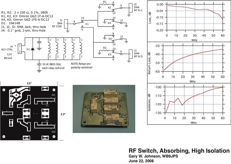
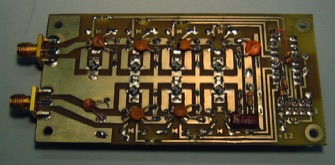
RF Switch
For the RF switch I used Omron G6Z series surface-mount RF relays, available through Mouser. They have very high isolation and excellent return loss specs. It’s driven by a single output bit on the USB Interface board.
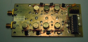
Digital Step Attenuator
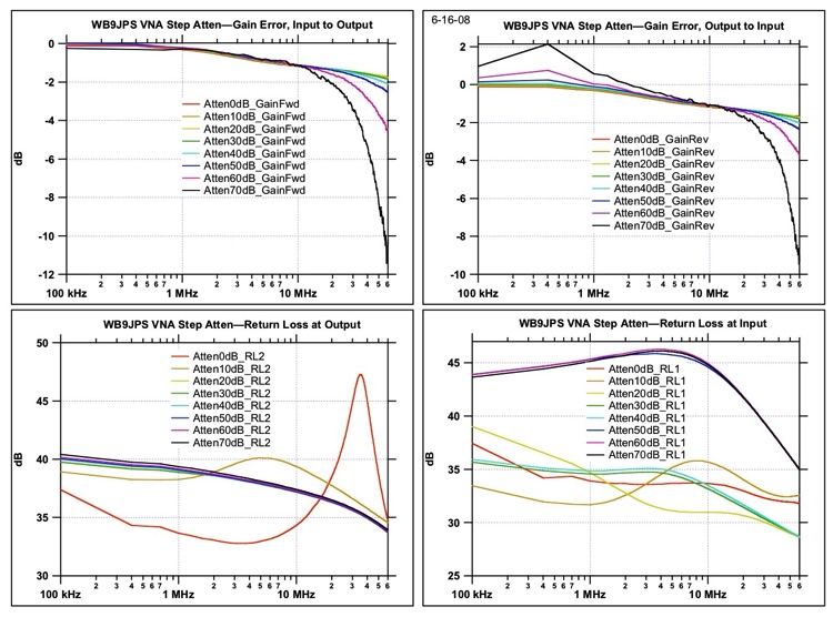
The reason for having a programmable attenuator in a VNA’s test set is to accommodate devices under test that have widely different forward and reverse gains, such as amplifiers. For this 0-70 dB step attenuator, I have a bunch of very nice Teledyne J412 DPDT TO-5 relays that have high isolation, low SWR, and are specified for use to 1 GHz. Thank heavens for Ebay, once again, where I found them for less than $10 each instead of the catalog price of $68. For attenuators, I’m using Minicircuits GAT-10 parts, which provide an accurate 10 dB in an SMT package. The final board is 2x4 inches.
Since the N2PK VNA interface supplies 3 bits for attenuation setting, a decoder is required. No simple logic device will do the job, since the objective is to turn on N relays where N is 0...7. A programmable logic device would do, or in my case I used a Z8 Encore microcontroller that I had laying around. By running its internal clock at 32 kHz, no RFI was detectable above -120 dBm.
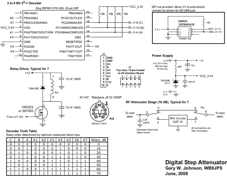
Even using microstrips and good relays, return loss was not as good as I wanted. Having high return loss generally improves VNA performance. Adding distributed capacitance and a series RC network did a pretty good job of tweaking the match up to 60 MHz. The cost was un-flat response, down about 2 dB at 60 MHz. After VNA calibration, this is of no consequence. I’m going to call this design irreproducible....
Wideband Bias Tee
To complete my test set, I designed a bias tee, which is useful when testing transistors or any other device that requires DC bias. See the Bias Tee page for more info.
LabVIEW Software Support for the VNA
Since I’m a LabVIEW guru, I couldn’t let the VNA project go without a good LabVIEW driver and application software. The current version requires the G8KBB USB interface. Because LabVIEW is platform-independent, there are some I/O driver options. Under Windows, you can use the G8KBB DLL as the driver, or NI-VISA. On the Mac, you must use NI-VISA. To look at the source code, you must have LabVIEW 2014 or later. The full version of LabVIEW is required. Please note that I am no longer supporting this application.
Mac or Windows. I offer full LabVIEW source versions for Windows and Macintosh OSX. Email if you would like a copy. There is a free community edition of LabVIEW available.
VNAView is a full-featured VNA application including calibration management, linear and log scanning, analysis and graphing of many computed parameters, Smith chart, RLC network fitting, and exporting data to tab-delimited text files. Since it’s LabVIEW, all the diagrams (source code) are there and you can instantly modify anything you want. Also, it’s easy to integrate the VNA application with other tests. The basic LabVIEW driver that I supply allows access to all VNA features including DDS setup, ADC acquisition, and setting digital output bits. Higher-level functions implement various VNA calibration algorithms including single-port reflection, reflection plus thru, and a full S-parameter test set. This document has some screenshots and notes: VNAView Info.pdf
My email: