Building Blocks for Flexibility... and Learning
A good way to learn how to build something complicated is to break it down into blocks that you understand, build those one at a time, and then link it all together. That’s my approach here. I had no expectation of building a highly-polished transmitter; I just wanted something that would provide CW/SSB capability and modest power (~50 W) on the HF bands. Most of all, I wanted to try my hand at basic RF design and have a good time! This project took about seven months.
Recycled Power Supply and Chassis
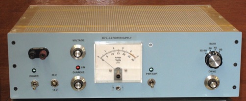
The enclosure you see above was originally an audio power amp that I built in my high school days. For the transmitter, I recycled the power transformer and huge filter caps, along with some of the mechanical stuff. The power supply provides 1.2 - 30 VDC at 4 A continuous (6 A max) with excellent regulation. It’s based on an LM317 with a moosey pass transistor, also lifted from the audio amp. This is a general-purpose power supply (see the binding posts on the panel), but with plenty of room for the transmitter modules. So if I decide to trash the transmitter later, this box will live on as a bench supply.
There’s another little transformer in there to provide other bias voltages: ±12 and ±5 at up to about 30 W, total.
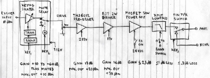
Like any transmitter, this one is basically a bunch of gain stages. The interesting parts are the keyed waveform shaping circuit, and maybe the sequencer and PIN diode T/R switch. We’ll look at each block in turn.
SPECIFICATIONS
Coverage: 3.5 to 30 MHz
> 35 Watts output, all bands
All harmonics < -60 dBc
T/R delay: 11 ms
Optimized keying bandwidth,
4.2 ms risetime
An Optimal Waveform Shaping Circuit
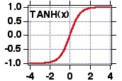
When you suddenly turn an RF signal on or off, you generate a wide-bandwidth transient. We usually call these key clicks. By slowing down the rise and fall times during keying, bandwidth (and clicks) are reduced. A mathematically optimal wave shape was derived by W9CF in this paper. That form is an error function. Such a function is easy to generate in real-time using DSP, but since I was doing an analog system, I used the fact that erfc() is approximately equal to the hyperbolic tangent function tanh(). That’s something that we can generate with a differential pair of transistors.
When the circuit is keyed, a ramp generator drives the tanh() converter, which produces the gentle transition. An LMH6505 linear variable-gain amplifier (VGA) shapes the RF signal from the exciter. It has a nice dynamic range, in excess of 60 dB up to at least 50 MHz, with very low distortion up to +10 dBm output. All I had to to was adjust the ramp rate to suit they keying rate, and carefully adjust the min/max voltages of the tanh() output to perfectly match the VGA dynamic range
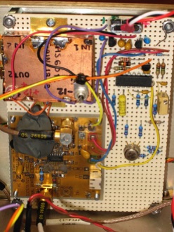
To provide complete muting and freedom from backwave, I used a small RF relay I had laying around. An analog switch would be better; just didn’t have one handy. In the board photo, there’s a blob of grey clay covering the relay to quiet it... Too much clatter when keying.
The shaper is followed by a pre-driver stage which is based on a high-performance DSL driver amplifier, a TSH6012. I wrote about its performance in a report, IQPRo_Performance_and_Wideband_Opamps.pdf. It’s capable of well over +20 dBm output with very low distortion out to 100 MHz. You can see it in its little copper shield in the photo at right. The LMH6505 is on an evaluation board and the tanh() generator is built on the main perfboard
Keying Waveform Measurements
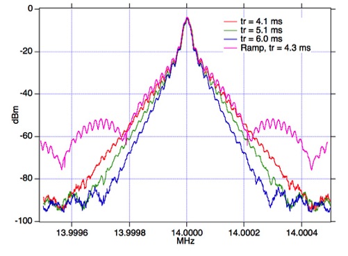
Besides a listening test, a good measurement for clean keying is to measure the power spectrum on a spectrum analyzer while generating a continuous stream of dits. I drove the keying shaper with a 10 Hz square wave while the analyzer scanned slowly over a 1 kHz bandwidth. Three different risetimes were tested, 4.1, 5.1, and 6.0 ms (ARRL typically recommends 5 ms for keying speeds up to at least 40 WPM). In the graph below, I also include the result when the shaping waveform is a simple RC exponential. You can see the much higher side lobes in that case. I ended up using a 5 ms risetime. Tuning away from the carrier of the optimized signal, it would be down about 80 dB just 300 Hz away. That makes me a “nice guy” in the CW portions of the bands. Mission accomplished.
One thing you do have to keep in mind is clipping in subsequent stages. We’re trying to produce a carefully-shaped waveform in the time domain, but if a downstream amplifier saturates prematurely, that flat-topping will result in key clicks and all our hard work is for nought. For that reason, my entire amplifier chain is linear, class AB, which is of course also suitable for SSB. I also adjust the drive to the final amplifier to a level that I know will keep it in its linear range; turning the drive up to “ten” is wrong; you get a couple extra watts, but defective keying. If I had a power amp with ALC, I would want to disable that feature because it, too, would distort this waveform.
A Two-Watt Wideband Driver Amplifier
Since my final amplifier needs at least 1 W input, I looked around for some options on a driver amplifier and decided on a fairly common broadband approach using bipolar transistors and binocular core transformers at the input and output. The circuit is loosely based on Motorolahttp://www.communication-concepts.com/content/AN779L/AN779_Application_Note.pdf application note AN779, the famous 20 W amplifier that you can buy as a set of parts from Communications Concepts, Inc. (CCI). I stole the first stage, used some generic CB transistors, and customized the transformers a bit to get “good enough” performance. This was my first attempt at a broadband amplifier of this type...
The first task was to try and optimize the winding of the transformers. For a constant turns ratio of 2:1, which is better: 2, 4, or 6 turns on the primary? Using 2843000202 binocular cores and 28 ga wire, I made three test articles and connected them via SMA connectors to my spectrum analyzer and tracking generator. Here are the frequency responses:
SPECIFICATIONS
Gain:
16 dB max, down 2 dB at 3
and 30 MHz
Max Power at 7 MHz:
+34.7 dBm, 3.0 W
Input return loss:
>11 dB, 1 to 30 MHz
(SWR < 1.2:1)
Distortion at 2 W output:
HD2 -48 dBc
HD3 -25 dBc
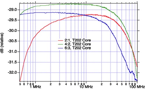
With too few turns, there is insufficient inductance and low frequency response suffers. With too many turns, a premature high-frequency rolloff occurs. The optimum appears to be the 4:2 turns ratio, so I went with that for the input transformer. It was flat within 0.3 dB from 3-30 MHz. The output transformer was a 4:3 ratio, plus a single turn for the feedback network.
Since the specified transistors were not on hand, I used some fairly generic low-cost devices (2SC2075), which meant that the input matching and feedback parameters from AN779 were invalid. So the tweaking began, attempting to flatten the response while maintaining a good input and output match. Having the tracking generator and analyzer, and a return loss bridge, were incredibly valuable.
Driver Amp Performance
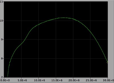
Here is the final frequency response, which is reasonably flat though not spectacular. Considering how un-flat the power amp turned out to be, this is more than sufficient.
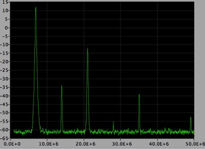
Full power at 7 MHz is about +34.7 dBm (2.95 W) when higher-order harmonics begin to jump up. At 2 W, HD2 = -48 dBc, HD3 = -25 dBc. Here is a typical distortion spectrum.
I never did get a current draw measurement. It runs off of 12 V and the PC board was fabricated by the Sharpie method. A full ground plane is used on the component side. There’s an overkill heatsink, about 2 x 3 inches and 0.5 inches thick and is the same size as the board. It runs comfy-cool and is totally stable and blowup-proof.
WA2EBY MOSFET Power Amplifier
After a market search, I decided on the WA2EBY power amplifier design, based on cheap IRF510 MOSFETs. This amplifier is featured in the ARRL Amplifier Classics book and some edition(s) of the Handbook. It’s also available in kit form from HF Projects as the HF Packer Amp; they also offer the amplifier board kit alone, which is much cheaper than the full kit. I built mine from the original article on double-sided copper clad, using the Sharpie method. A full ground plane is highly desirable for any RF design, and especially so for power amplifiers.
My general board fabrication procedure is this: First, draw the wiring side layout on 0.1-inch grid paper. Second, drill all the through holes. I use a Moto-Tool in its drillpress stand and HSS drill bits from #75 on up. Third, mark the holes on the component (ground plane) side that do not connect to ground. These I disconnect from the ground plane using Stahler drill mill cutters, which are no longer available. You can also use a ball-end cutter on the Moto-Tool to remove the copper immediately around the hole. Fourth, I paint the ground plane with fast-drying auto primer, which is the fastest way to entirely cover the board with resists. Fifth, I draw the pattern with a fresh black Sharpie. Finally, drop it in etchant. I like ammonium chloride because it’s clear. To remove the resist, wash with lacquer thinner. Parts that have a connection to ground are soldered directly to the ground plane on the component side. This avoids an extra wire path through the board.
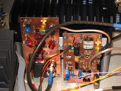
Below is the complete power amplifier (left) and 2-W driver amplifier (right). I used this peculiar orientation because it made access to the IRF512 tabs very easy when (not if) they need replacement.
I run my amplifier on 24 VDC rather than 28 to give it a little bit more margin on breakdown voltage. To adjust bias, I have a 0.1 ohm resistor in the power return lead, and I set the bias at about 10 mA for each transistor. Performance-wise, distortion is low up to a total current of nearly 4 A, so I generally tune up my transmitter by adjusting the Drive pot for about 3.5 A. Heat has not been a problem at all during normal CW operation. I do limit my testing duty cycle so as not to push my luck. My heatsink is very large but thermal conductivity within the devices is the weak point.
The only failure I’ve had is when driving the amplifier into a lowpass filter that is too low in frequency. In that case, the SWR is infinite and both IRF510s fail shorted. Running with a poorly-tuned transmatch has not been a problem, but I cautiously do my initial tuning with minimal drive
Transmitter Lowpass Filter Board
After the power amplifier, we have a set of fifth-order LC Chebychev lowpass filters. These are pretty ordinary designs. My filter design tool is a very expensive commercial one that I have access to at work called Filter Solutions from Nuhertz. For this application, it’s generally good enough to use the tables in the ARRL Handbook, or just copy some else’s design.
I fabricated my filter board on double-sided copper clad using the Sharpie method. Toroids are the 68 size to handle >100 W and all capacitors are 500 V dipped mica. Relays are Axicom V23079D1003B301, available from Mouser for about $2.50 each. They are among the few small, affordable, relays that I’ve seen that have real RF specifications to 900 MHz and 1 kV/2A contact rating. Certainly good enough for my purposes.
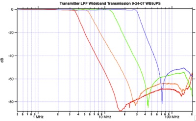
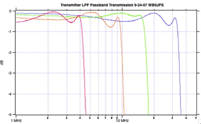
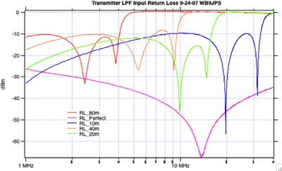
LPF Performance
Here are the transmission loss measurements and input return loss measurements. I like to do a wideband test, way out into the VHF range, just to see how good my construction techniques and components are. As you can see, these simple filters provide >50 dB rejection all the way out to 200 MHz. That’s the ground plane at work, and also the fact that these filters are all-pole designs as opposed to elliptic topologies with transmission zeros (capacitors in parallel with the inductors). In those filters, you often see poor attenuation at high frequencies due to non-ideal component behavior.
A Solid-State T/R Switch Using PIN Diodes
The final board in my transmitter is the T/R switch. Since my power level is below 100 W, it’s feasible to use ordinary power diodes as RF switching devices. Wes Hayward, W7ZOI, wrote a nice article on this in the May, 1995 issue of QEX, “Electronic Antenna Switching.” If you have copy of his excellent book, Experimental Methods in RF Design, it’s included on the CDROM. I simply used the final design in that article, with some minor modifications.
The one thing I added, as suggested in the article, is a shunt switch at the receiver port. This made a big reduction in leakage from transmitter to receiver at frequencies above about 10 MHz. I included an onboard power supply made from a couple of small 7.5 VAC transformers I had in my junkbox.
As usual, I fabricated my filter board on double-sided copper clad with a full ground plane using the Sharpie method.
TR Switch Performance
The 9 V bias supply has to be well filtered. In the article, Wes used regulated 12 VDC from the transmitter supply. I may switch to that, because hum and noise on my 9 V supply does leak into the receive signal. Using a 10,000 uF filter cap makes it negligible compared to band noise, but still above the receiver’s noise floor.
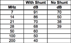
Here is the transmit to receive isolation with and without the final shunt PIN switch on the receiver port. For reference, an isolation of 50 dB at 7 MHz is equivalent to 0.75 pF. That means the “off” capacitance of the diodes is quite low, and the stray capacitance is also very low.
This data was taken with the T/R switch on the bench under small-signal conditions. When used with the completed transmitter and with the power amplifier running full power (about +48 dBm), power at the receiver port was as higher than predicted. For instance, at 14 MHz, the receiver sees -21 dBm, or an isolation of 69 dB. Other stray coupling methods were at work. Still, that’s only 10 microwatts of leakage, which any receiver can handle gracefully.
Passband losses
From antenna port to receiver port From transmitter port to antenna port antenna port
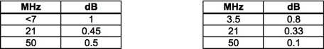
Losses are acceptably low, especially for the HF bands. At 3.5 MHz, most of the loss is from the 22 nF coupling capacitors that I used. Paralleling a couple would have improved that.
Switching time is in the sub-microsecond domain when one of the transistors is turning on, which is the direction that brings a pair of PIN diodes into conduction. When the transistor turns off, the 100k resistor must charge one or more 22 nF capacitors, with a time constant of 2.2 ms. However, the diodes are effectively off almost immediately since the forward bias disappears long before the reverse bias has built up. The only reason for high reverse bias is to reduce leakage capacitance to the lowest possible level. So this system also turns off in a few microseconds.
Microcontroller T/R Sequencer Board
Any transceiver system has several items that must be switched in the proper sequence when transitioning between transmit and receive mode. For my rig, I decided to use a microcontroller to provide a programmable sequence of events on a series of digital outputs in response to the key input.
I chose the Zilog Z8 Encore XP series because:
They come in DIP packages, as well as surface mount
The CPU family includes a wide variety of I/O types, and an on-chip clock
The evaluation board is cheap ($40) and uses a USB programming pod
The evaluation kit comes with a full ANSI C compiler
Since I’m about 100X more productive in C than assembler, the free compiler was the clincher for this deal. CPU performance was not much of an issue since we’re only trying to do simple digital timing at the sub-milliseocond level.
Getting the evaluation kit going was pretty easy after reading the documentation. I actually used my MacBook, which is Intel-based, booted up in Windows XP, as the development system. That worked great. It didn’t work from Parallels, a virtual machine that allows most Windows applications to operate transparently under the regular Mac OS. Must be something funny about the USB support. Anyway, the example code that Zilog supplies was all I needed to get going.
I started out by listing the items to be controlled (T/R switch, receiver mute, VFO T/R frequency switch, etc.) and assigned delay times for each one. Times are different for T-to-R and R-to-T modes. The microcontroller timer resolves 0.1 ms, which makes it easy to dial in the delays precisely while testing the overall rig.
Program Design
Since this microcontroller has nothing else to do, it’s main idle loop simply polls the key input, waiting for it to change state. The other thing that goes on continuously is the handling of interrupts from one of the counter-timers. The counter is set up to divide the on-chip clock (5.70 MHz) by 570 to produce an interrupt every 0.1 ms. When we need to start measuring elapsed time, we set a variable to zero and then increment it at each interrupt until the desire time is reached.
The program is a state machine with three states:
1. Key down: The key input just transitioned to the transmit mode. The code waits for a series of intervals to elapse, and sets output bits at desired times.
2. Key up: Similar to the key down state, but transitioning to receive mode.
3. Idle: The key state is not changing; it could be in either state. The code polls for a change of key state.
Sequencer Performance
Timing jitter was plus or minus 50 microseconds (within one tick of the timer). I did have to adjust some of the times, especially the one associated with the sidetone so that its sound occurred at exactly the same time that carrier was produced. This project was so easy to build and the code was so easy to create and modify that I’ll be looking forward to another application in the near future.
In Closing...
So that's a wrap on my experimental CW transmitter. I did in fact get it on the air with its mighty 40W and made a number of contacts using a low dipole. It was a flashback to my novice days with my HW-16, which had similar features!